While in the Arduino, a lot of the ins and outs of the real functioning of the chips has been made easier, when we start making the change into AVR C coding, we will have to start understanding the real thing that is an ATMega chip !
One of the things is start understanding all the peripherals that the chip has, which means going beyong the ON-OFF digital function of a pin.
That can include( depending on the chip): Digital I/O -- On or Off; Parallel signals; Pulse-width-modulated logic signals; Counters and timers
Analog I/O -- Voltages; Comparators; Analog-to-digital converters (ADCs); Digital-to-analog converters (DACs).
But why do we need ADC's ?!? Well, a lot of sensors that are used in Electronics(and Robotics) give output voltages in the form of potential differences in voltages; We can attach an interrupt to the conversion, so that we dont need to constantly keep checking on it; We can also use it with potentiometers to control a variable depending on the value's reading, and many other applications im sure you will think of !
So lets start with the Analogue to Digital converters that the ATMega has . As far as Analogue to Digital Inputs go, it states we have available 6 channels with a 10 bit resolution ! This means that you can distinguish between two readings which have a difference of Reference Value/210 . The max value is broken up into 210-1 = 1023 parts and if you have a reference of say 5V, you can distinguish between readings 4.88mV apart.
The ADC is a 10-bit ADC, ie, it provides measurements in the range 0 to 1023. Situated at the entrance of the input is the Ground , so the ADC provides a value of 0.If the voltage at the input matches the reference voltage ( not quite), then it passes a value of 1023. If the 10-bit resolution is not needed, it is possible to restrict the output by a configuration register so that a easy access to the 8 most significant bits is possible.
As with many analog circuits, the ADC is also subject to noise . This means that one should not assume that the ADC input at a constant voltage outputs always the same constant value. A "trembling" of the least significant 2 bits is not unusual. Should be emphasized again at this point, the quality of the reference voltage. This quality will significantly change the quality of the results. The circuit of AREF with a suppressor filter capacitor is the absolutely necessary to obtain a reasonably acceptable reference voltage.If this is not sufficient, then by oversampling you can increase the quality of measurement. For this purpose, several measurements are made to form an average.

- ADMUX (ADC Multiplexer Selection Register),
- ADCSRA (ADC Control and Status Register A),
- ADCSRB (ADC Control and Status Register B),
- DIDR0 (Digital Input Disable Register 0),
- ADCL (ADC Data Register – Low)
and
- ADCH (ADC Data Register – High).

Reference voltage is controlled by REFS1 and REFS0. AREF is used by default, but there are also other options available (more about it soon) ! (see graphic)
0 -The result is right-aligned in the registers ADCH / ADCL. The 8 least significant bits of the result are stored in ADCL. The remaining 2 bits of the result are stored in register ADCH in bits 0 and 1.
1 - The result is left-aligned in the registers ADCH / ADCL. The 8 most significant bits (MSB) of the result are stored in ADCH. The remaining 2 low order bits (LSB) are stored in the register ADCL in bits 6 and 7.
ADC Data Register
If conversion is finished, the measured value is in these two registers. Of ADCH only the two least significant bits are used. It must always be read both registers, and always in the order: ADCL, ADCH . The actual measured value is then given by:
x = ADCL; / / with uint16_t x
= x + ( ADCH << 8 ) ; / /(LSB / MSB order, and in two lines to ensure / / C operator precedence)
or
x = ADCW; / / depending on the AVR and x = ADC (see avr / ioxxx.h)
MUX0 to MUX3 are used to select which input channel you wish to read. (The values 0000 to 0101 allow you to select ports PC0 to PC5, while the reserved values of 1110 and 1111 allow you to select 1.1V and 0V.
ADCSRA and ADCSRB are used to control the Analogue to Digital conversion .

ADCSRB - ACME - - - ADTS2 ADTS1 ADTS0
Read/Write R R/W R R R R/W R/W R/W
Initial Value 0 0 0 0 0 0 0 0
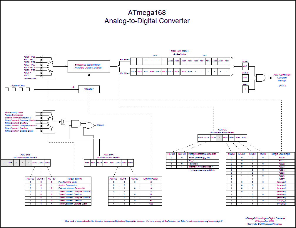
This graphic gives you get a better birds eye view and and should help understand better the whole process ( Courtesy of web.alfredstate.edu )
CLICK FOR BIGGER PICTURE
* to be Continued...
No comments:
Post a Comment
Feel free to contact me with any suggestions, doubts or requests.
Bless