| 1-Wire | I²C* | SMBus™ | SPI™ | MicroWire/PLUS™ | M-Bus (EN1434) | CAN (ISO11898) | LIN Bus | |
| Network Concept | single master, multiple slaves | multiple masters, multiple slaves | multiple masters, multiple slaves | single master, multiple slaves | single master, multiple slaves | single master, multiple slaves | multiple masters, multiple slaves | single master, multiple slaves |
| Number of Signal Lines | 1 (IO) | 2, (SCL, SDA) | 2, (SMBCLK, SMBDAT) | 4, (active-low CS, SI, SO, SCK) | 4, (active-low CS, DI, DO, SK) | 2 (lines can be swapped) | 2 (CAN_H, CAN_L, terminated) | 1 (LIN) |
| Optional signals | N/A | N/A | SMBSUS#, SMBALERT# | N/A | N/A | N/A | 2nd GND, Power, Shield | N/A |
| Network Size | Up to 300 m (with suitable master circuit) | Limited by max. 400pF buscapacitancerequirement | Limited by max. 400pF bus capacitance requirement | N/A (circuit board level) | N/A (circuit board level) | Max. 350m per segment of max. 250 slaves; max. 180nF | 40m @1M bps1000m @ 50k bps(example) | Up to 40m, max. 10nF total load |
| Network Interface | open drain, resistive or active master pull-up | open drain, resistive or active master pull-up | open drain, resistive or active master pull-up | Push-pull with tristate | Push-pull with tristate | M to S:voltage drive S to M: current load | Differential open drain/source or open coll./emitter | open drain, resistive master pull-up |
| Network Voltage | From 2.8 to 6.0 V, device specific | From 1.8 to 5.5V, device specific | 2.7V to 5.5V | From 1.8V to 5.5V, device specific | From 1.8V to 5.5V, device specific | ~40V | VDD-VD (diodedrop); ~4.5V max. | 8 to 18V |
| Logic Thresholds | Vary with network voltage | Fixed level: >1.5V, >3.0 V VDD-related level: <30>70% of VDD | <0 .8v=".8v">2.1V | VDD-related level: <20>70% of VDD(inconsistent) | Fixed level: <0 .8v=".8v">2.0V; VDD-related level: <20>70% (80%) of VDD (inconsistent) | Master to slave: 24V, 36V nominalSlave to master: <1 .5ma=".5ma">11mA | Differential: <50mv recessive="recessive">1.5V (dominant); driver specification | VDD-related level: <20>80% of VDD (driver spec.)<40>60% of VDD (receiverspec.) |
| Transmission | LS bit first, half-duplex | MS bit first plus Acknowledge bit, half-duplex | MS bit first plus Acknowledge bit, half-duplex | MS bit first, full-duplex | MS bit first, full-duplex | LS bit first,half-duplex, acknowledge response | MS bit first, half-duplex | LS bit first, half-duplex |
| Address Format | 56 bits | 7 bits, (10 bits defined but not implemented) | 7 bits, (10 bits defined but not implemented) | N/A | N/A | 8 bits (primary address), 64 bits (secondary address) | Message identifier 11 bits (standard format), 29 bits (extended format) | Message identifier 8 bits, including 2 parity bits |
| Network Inventory | Automatic, supports dynamic topology change | N/A; slave addresses hard-coded in firmware | ARP, Address Resolution Protocol (Rev. 2.0 only) | N/A; slave select (active-low CS) hard-coded in firmware | N/A; slave select (active-low CS) hard-coded in firmware | Automatic | N/A; message-based protocol, not address based | N/A; message-based protocol, not address based |
| Gross Data Rate | Standard: ~0 to 16.3k bps Overdrive: ~0 to 142k bps) | Standard: ~0 to 100k bps; Fast: ~0 to 400k bps; High-Speed: ~0 to 3.4M bps | 10k to 100k bps | ~0 to ~10 M bps (device specific) | ~0 to ~5 M bps (device specific) | 300, 2400, 9600 bps | ~0 to 1M bps | ~1k to ~20k bps |
| Access Time | Standard: ~ 5.4ms Overdrive: ~0.6ms (at maximum speed) | Standard: ~95µsFast: ~23µs(at maximum speed) | ~95µs @ 100k bps | N/A | N/A | Primary address, 2400 bps: 13.75ms (short frame), 27.5ms (long frame) | At 1M bps 19µs (standard) or 39µs (extended) from start of frame to 1st data bit | At 20k bps 1.7ms from start of frame to 1st data bit |
| Data Protection | 8-bit and 16-bit CRC | N/A | PEC Packet Error Code (Rev.1.1, 2.0) | N/A | N/A | Even parity, check sum, frames | 15-bit CRC, frames, frame acknowledge | Check sum, frames |
| Collision Detection | Yes, through non-matching CRC | Yes (multi-master operation only) | Yes (Rev. 2.0 only) | N/A | N/A | Yes ("medium" and "strong" collisions) | Yes: CSMA/CD | Yes, through check sum |
| Slave supply | Parasitic (typical), VDD(exception) | VDD only | VDD only | VDD only | VDD only | Parasitic and/or local supply | VDD only, local or remote source | Parasitic only |
Saturday, 8 September 2012
Serial Digital Data Networks
Wednesday, 5 September 2012
Pinguino 32 Olimex boards PWM pins info !
As i had trouble finding this information which will be the subject of this post myself, i decided to leave a note about it it here in case someone gets "lost" on it as well !
The Olimex boards PIC32 PWM pins info !
Digital Pins D0, D1 and D2 are the one on which you can use analogWrite ( and PWM as well as theres a PWM_set_frequency(u32 freq), /*
PWM_set_frequency--------------------------------
@param: frequency in hertz (range 3kHz .. 12MHz)
PB is Peripheral Bus Clock
let's say p = TMR Prescale Value
PWM Period = (PR + 1) * TPB * p
so (PR + 1) = PWM Period / (TPB * p)
but PWM Period = 1 / PWM Frequency
so (PR + 1) = (1/PWM Frequency) / (1/TPB * p)
and (PR + 1) = FPB / (PWM Frequency * p)
then (PR + 1) = FPB / PWM Frequency / p -------------------------------- ------------------ PR3+1 calculation
_pr3_plus1 = GetPeripheralClock() / freq; // FOSC / PWM Frequency
Timer3 prescaler calculation
PR3 max value is 0xffff, so PR3+1 max value is 0x10000 = 65536
highest prescaler value is 256
256 * 65536 = 0x1000000 = 16777216 :*/
PWM_set_dutycycle(u8 pin, u16 duty), /* PWM_set_dutycycle
1. Set the PWM period by writing to the selected timer period register (PRy).
2. Set the PWM duty cycle by writing to the OCxRS register.
3. Write the OxCR register with the initial duty cycle.
4. Enable interrupts, if required, for the timer and output compare modules. The output
compare interrupt is required for PWM Fault pin utilization.
5. Configure the Output Compare module for one of two PWM Operation modes by writing
to the Output Compare mode bits, OCM<2:0> (OCxCON<2:0>).
6. Set the TMRy prescale value and enable the time base by setting TON
(TxCON<15>) = ‘1’. */
PWM_set_percent_dutycycle(u8 pin, u8 percent) /* PWM_set_percent_dutycycle--Set a percentage duty cycle, allowing max 100 PWM steps.Allowed range: 0..100The duty cycle will be set to the specified percentage of the maximum for the current PWM frequency.Note: The number of available PWM steps can be lower than 100 with (very) high PWM frequencies-- */

Relying with my limited experience with the PIC16F family, i went digging for info on the code and found something that helped me, at least for now !
So to clear that ill leave an excerpt of the pwm.c, with some additional comments for those who might interest:
#if defined(PIC32_PINGUINO) || defined(PIC32_PINGUINO_OTG)
	switch (pin)
	{
		case 2:
			TRISDSET=0x10; /* D2 in the Board, RD4 pin which is also connected to the button (see schematics); 0b10000 in binary */
			TRISDCLR=0x01;
			OC1CON=0;
			OC1R=setpoint;
			OC1RS=setpoint;
			OC1CON=0x000E; /*Binary 1110 activates OCM's bit 2-0, where 1110 = PWM mode on OCx; and bit 3-0 1110 OCTSEL: Output Compare Timer Select bit where 1 = Timer3 as the clock source for this OCMP module */
			OC1CON|=0x8000; /* Binary 1000000000000000 is bit 15 ON: Output Compare Peripheral On bit(1), where 1 = Output Compare peripheral is enabled and 0 = Output Compare peripheral is disabled */
			return 1;
			break;
		case 1:
			TRISDCLR=0x08; /* D1 in the Board, RD3 pin, 0b1000 in binary . This Pin is also TX1*/
			OC4CON=0;
			OC4R=setpoint;
			OC4RS=setpoint;
			OC4CON=0x000E;
			OC4CON|=0x8000;
			return 1;
			break;
		case 0:
			TRISDCLR=0x04;  /* D0 in the Board, RD2 pin, 0b100 in binary where 0 is a number. This Pin is also RX1 */
			OC3CON=0;
			OC3R=setpoint;
			OC3RS=setpoint;
			OC3CON=0x000E;
			OC3CON|=0x8000;
			return 1;
			break;
		default:
			return 0;
	}
#endif
I have had both this and the DIP DIY version with the PIC32MX250F128B, with 128k of flash and 32k of RAM, 17 I/O, 2 UART etc , that with a works with a 8 Mhz crystal for a finally system frequency of 40 Mhz.
As the Pinguino board from Olimex uses an IDE that is "Arduino Compatible" but with a PIC32MX440F256H , you can imagine how handy that can be ! The specs that Olimex got us used to makes it worth it all the more !
Things like DCDC power supply allow power supply voltage from 9 to 30V DC, Li-Ion rechargeable battery power supply option with BUILT-IN on-board charger, so when you attach battery it is automatically charged and kept in this state until the other power source is removed (and it AUTOMATICALLY will power the board); original Arduino design had flaw and the connectors were not spaced at 0.1" this make perfo board use impossible, So this has a connector on 0.1" !!; UEXT connector; RTC - Real Time Clock.; NOISE IMMUNE design. and last but least the chip itself which is a PIC32MX440F256H @ 80 Mhz microcontroller with 256KB Flash and 32KB RAM
Of course you can use the Arduino C++ style with:
int led = 13;
void setup() {
pinMode(led, OUTPUT);
}
void loop() {
digitalWrite(led, HIGH); // turn the LED on (HIGH is the voltage level)
delay(1000); // wait for a second
digitalWrite(led, LOW); // turn the LED off by making the voltage LOW
delay(1000); // wait for a second
BUT ... Ill leave you also a more direct way of blinking leds, released by Olimex itself ( they have some good examples, though mainly related to their MODboards). The code been partially commented by me just to help in our quest !
/*
		PIC32-PINGUINO
		Blinks both LEDs (Green and Yellow)

    If you have any questions, email
    support@olimex.com

    OLIMEX, JULY 2012
    http://www.olimex.com
*/

#if ( defined(PIC32_PINGUINO_OTG) || defined(PIC32_PINGUINO) || defined(PIC32_PINGUINO_MICRO) )

	//Definitions for
	// -- PIC32-PINGUINO
	// -- PIC32-PINGUINO-OTG
	// -- PIC32-PINGUINO-MICRO

	#define BUTTON1INIT TRISDbits.TRISD0 = 1

	/*YELLOW LED is PORTD1, which is connected directly and exclusively into a led on the board */
	#define YLEDINIT   TRISDCLR = 0x02;
	#define YLED1         PORTDSET = 0x02;
	#define YLED0         PORTDCLR = 0x02;
	#define YLEDSWITCH    PORTD   ^= 0x02;

	//GREEN LED is D13 in board , PORTG6 pin / 0b1000000 on chip
#define GLEDINIT TRISGCLR = 0x40; /* Clearing the Port/bit */
	#define GLED1 		    PORTGSET = 0x40; /* Setting the bit */
#define GLED0 		    PORTGCLR = 0x40;  /* Clearing the bit */
	#define GLEDSWITCH          PORTG   ^= 0x40; /* Toggling the bit/led */

	#define YELLOW 0
	#define GREEN  1
	#define BOTH   2
#endif

//Blinks an LED five times - mode is YELLOW, GREEN or BOTH
void blinkled(unsigned char mode);


void setup() {
    // put your setup code here, to run once:
    YLEDINIT;  /* Clearing the Port/bit */
    GLEDINIT; /* Clearing the Port/bit */
    }

void loop() {
    // put your main code here, to run repeatedly:
    blinkled(GREEN); /* Using the function below created ! */
    blinkled(YELLOW);
    blinkled(BOTH);


}

void blinkled(unsigned char mode)
{
	//Turn off all LEDs
	YLED0;  /* Clearing the bit */
	GLED0;  /* Clearing the bit */


	char i;

	// Blink
	switch(mode)
	{
		case YELLOW:
			for(i=0; i<10;i++)
			{
				YLEDSWITCH;/* Toggling the bit/led */
				delay(100);
			}
			break;

		case GREEN:
			for(i=0; i<10;i++)
			{
				GLEDSWITCH;/* Toggling the bit/led */
				delay(100);
			}
			break;

		case BOTH:
			for(i=0; i<10;i++)
			{
				YLEDSWITCH;/* Toggling the bit/led */
				GLEDSWITCH;/* Toggling the bit/led */
				delay(100);
			}
			break;
	}
}

Reference :
- Pinguino's Website and Forum
http://www.pinguino.cc/
- Compatibility Pinguino vs. Arduino
http://wiki.pinguino.cc/index.php/Compatibility
- Pinguino's blog (Info about the DIY of the PIC32MX or the 8Bit with PIC18F)
http://blog.pinguino.cc/
- Documentation about the DIY of the PIC32MX And the IDE download
http://code.google.com/p/pinguino32/downloads/list
Olimex Industrial-Grade board
https://www.olimex.com/dev/pic32-pinguino.html
Tuesday, 28 August 2012
Timers ( AVR ) : The theory behind it
*As the Analog to Digital tutorial is going take longer than i estimated at first, i'll leave you another introductory on Timers...
While the use of delay() can be useful for simple tasks, will also keep the uC busy until it it finishes waiting !
While the use of delay() can be useful for simple tasks, will also keep the uC busy until it it finishes waiting !
So, we are going to have a look at the timers of an AVR chip !
The AVR has an interesting counting circuit. This circuit has 2 inputs and one output. If you tie it into the Tn pin it will count the pulses on the pin (this is referred to as a counter on the datasheet). If you tie it into the AVRs internal(or external) clock you now have a timer. If you tie the counter to the output you will get an Pulse Width Modulator signal on the OCnx pin.


- 2nd ( blue) shows the pulses coming out of the pre-scaler (clk_tn or clk/8). In our example the pre-scaler is set to 8 so, it divides the clk(red) by 8.
- 3rd shows the TCNTn (basically the count). The TCNTn updates on the falling edge of the pulse coming out of the pre-scaler. On our first pre-scaler pulse ( blue) our TCNTn is TOP-1 (or 254). On our 2nd pre-scaler pulse( blue) our TCNTn goes to TOP (or 255). Now, on our third pre-scaler ( blue) pulse the TCNTn register overflows back to the BOTTOM (or 0) because it was at its TOP value on the previous pulse. On our 4th pre-scaler pulse ( blue) the TCNTn register gets incremented again this time to BOTTOM + 1 (or 1).
- The 4th shows the TCNTn register again. The only difference is that it shows TCNTn register in a Phase Corrected PWM pattern, which means that it counts up until it hits the TOP and then start to count down until it hits the BOTTOM . * More about this in the PWM tutorial.
- The 5th line ( green) shows us the TOVn (Timer Overflow bit). This bit is set the first time that a timer overflows. Or in other words the first time that the timer goes from its TOP state to its next state (BOTTOM in the 3rd line or, TOP -1 in the 4th line).
- The 6th line shows the OCRnx register. This register deals with the PWM. The only thing that it is showing, is that the OCRnx register can only be updated when an TOVn (timer overflow) condition happens. * More on the OCRnx register in the PWM section.1

.
In other words, the pre-scaler counts the number of input pulses (from the internal clock or from external sources) and when the number reaches the preset number (0, 8, 32, 64, 128, 256 or 1024) it generates a pulse of its own. This can be seen in Figure 2 (above) which divides the input by 8. This is needed because the AVR only has an 8bit and a 16bit register
Now the maths :
What if we use a pre-scaler of (lets say ) 1024 ?!

As a taster, ill leave you a simple code here for a blinky, to use on the Arduino Board ( as Port B 5/ pin 13 is used for led ); I included a commented pre-scaler at 1 just for reference
In other words, the pre-scaler counts the number of input pulses (from the internal clock or from external sources) and when the number reaches the preset number (0, 8, 32, 64, 128, 256 or 1024) it generates a pulse of its own. This can be seen in Figure 2 (above) which divides the input by 8. This is needed because the AVR only has an 8bit and a 16bit register
Now the maths :
The math is fairly simple:
Pre-scaler = Pre-scaler / Pre-scaler
And
Pre-scaler = Pre-scaler * Pre-scaler
And don't forget the old
Frequency = Period / Time
Then, to calculate how long would take to the AVR to generate a pulse ?!?
Frequency = Period / Time
Period / Frequency = Time
Time = Period / Frequency
Time = 16bit_register_size / System_clock_speed
Time = 0xFFFF(aka 65535 )/ 16Mhz
=
Time
Pre-scaler
= Pre-scaler *
Pre-scaler
Pre-scaler =
Time * 1024
= Pre-scaler
In the datasheet says that it is recommended that all external sources are limited to system clock / 2.5 . The Arduino runs at 16Mhz therefore
you are only able to reliably measure up to an 6.4Mhz signal or less.
Also, starting the pre-scaler will start the timer, so I recommend setting the pre-scaler bits last when setting up your timer in your program.
Now, i will leave you with a handy reference table, that i am sure will be helpful many a time !!
Now, i will leave you with a handy reference table, that i am sure will be helpful many a time !!
As a taster, ill leave you a simple code here for a blinky, to use on the Arduino Board ( as Port B 5/ pin 13 is used for led ); I included a commented pre-scaler at 1 just for reference
#include <avr/io.h>

int main (void)
{
  unsigned char ElapsedTime = 0; // Make a new counter variable and initialise to zero

  DDRB |= (1 << 5); // Set LED as output
  TCCR1B |= (1 << CS10); // Set up timer at Fcpu/1

  for (;;)
  {
    // Check timer value in if statement, true when count matches 1/2 second
    if (TCNT1 >= 16000)
    {
      TCNT1 = 0; // Reset timer value
      ElapsedTime++;

      if (ElapsedTime == 244) // Check
      {
        ElapsedTime = 0; // Reset counter variable

        PORTB ^= (1 << 5); // Toggle the LED
      }
    }
  }
}
Reference :
- AVR130: Setup and Use the AVR Timers
http://www.atmel.com/Images/doc2505.pdf
- Reference table
http://www.gammon.com.au/forum/?id=11504
- Timers and counter
http://embedded-lab.com/blog/?p=902
Saturday, 25 August 2012
Beyond the GPIO Pins : Peripherals & Intro to ADC
While in the Arduino, a lot of the ins and outs of the real functioning of the chips has been made easier, when we start making the change into AVR C coding, we will have to start understanding the real thing that is an ATMega chip !
One of the things is start understanding all the peripherals that the chip has, which means going beyong the ON-OFF digital function of a pin.
That can include( depending on the chip): Digital I/O -- On or Off; Parallel signals; Pulse-width-modulated logic signals; Counters and timers
Analog I/O -- Voltages; Comparators; Analog-to-digital converters (ADCs); Digital-to-analog converters (DACs).
But why do we need ADC's ?!? Well, a lot of sensors that are used in Electronics(and Robotics) give output voltages in the form of potential differences in voltages; We can attach an interrupt to the conversion, so that we dont need to constantly keep checking on it; We can also use it with potentiometers to control a variable depending on the value's reading, and many other applications im sure you will think of !
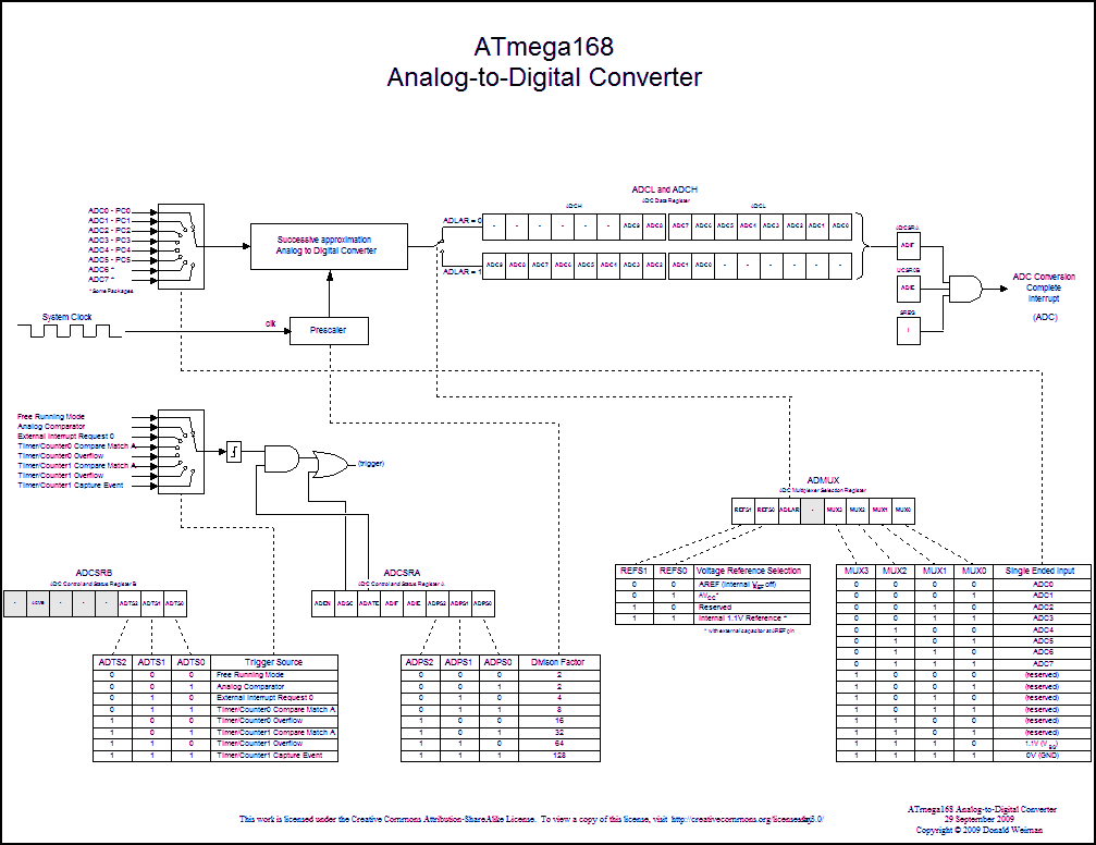
So lets start with the Analogue to Digital converters that the ATMega has . As far as Analogue to Digital Inputs go, it states we have available 6 channels with a 10 bit resolution ! This means that you can distinguish between two readings which have a difference of Reference Value/210 . The max value is broken up into 210-1 = 1023 parts and if you have a reference of say 5V, you can distinguish between readings 4.88mV apart.
The ADC is a 10-bit ADC, ie, it provides measurements in the range 0 to 1023. Situated at the entrance of the input is the Ground , so the ADC provides a value of 0.If the voltage at the input matches the reference voltage ( not quite), then it passes a value of 1023. If the 10-bit resolution is not needed, it is possible to restrict the output by a configuration register so that a easy access to the 8 most significant bits is possible.
As with many analog circuits, the ADC is also subject to noise . This means that one should not assume that the ADC input at a constant voltage outputs always the same constant value. A "trembling" of the least significant 2 bits is not unusual. Should be emphasized again at this point, the quality of the reference voltage. This quality will significantly change the quality of the results. The circuit of AREF with a suppressor filter capacitor is the absolutely necessary to obtain a reasonably acceptable reference voltage.If this is not sufficient, then by oversampling you can increase the quality of measurement. For this purpose, several measurements are made to form an average.

- ADMUX (ADC Multiplexer Selection Register),
- ADCSRA (ADC Control and Status Register A),
- ADCSRB (ADC Control and Status Register B),
- DIDR0 (Digital Input Disable Register 0),
- ADCL (ADC Data Register – Low)
and
- ADCH (ADC Data Register – High).

Reference voltage is controlled by REFS1 and REFS0. AREF is used by default, but there are also other options available (more about it soon) ! (see graphic)
0 -The result is right-aligned in the registers ADCH / ADCL. The 8 least significant bits of the result are stored in ADCL. The remaining 2 bits of the result are stored in register ADCH in bits 0 and 1.
1 - The result is left-aligned in the registers ADCH / ADCL. The 8 most significant bits (MSB) of the result are stored in ADCH. The remaining 2 low order bits (LSB) are stored in the register ADCL in bits 6 and 7.
ADC Data Register
If conversion is finished, the measured value is in these two registers. Of ADCH only the two least significant bits are used. It must always be read both registers, and always in the order: ADCL, ADCH . The actual measured value is then given by:
x = ADCL; / / with uint16_t x
= x + ( ADCH << 8 ) ; / /(LSB / MSB order, and in two lines to ensure / / C operator precedence)
or
x = ADCW; / / depending on the AVR and x = ADC (see avr / ioxxx.h)
MUX0 to MUX3 are used to select which input channel you wish to read. (The values 0000 to 0101 allow you to select ports PC0 to PC5, while the reserved values of 1110 and 1111 allow you to select 1.1V and 0V.
ADCSRA and ADCSRB are used to control the Analogue to Digital conversion .

ADCSRB - ACME - - - ADTS2 ADTS1 ADTS0
Read/Write R R/W R R R R/W R/W R/W
Initial Value 0 0 0 0 0 0 0 0
This graphic gives you get a better birds eye view and and should help understand better the whole process ( Courtesy of web.alfredstate.edu )
CLICK FOR BIGGER PICTURE
* to be Continued...
Wednesday, 22 August 2012
Tarte de Framboesas aka Raspberry Pi
Last delivery brought Raspberry Pi and a PIC16F887 Dip.
For those willing to use a translator on their browser, heres a portuguese blog on the RP board !!
Also make sure you check wiringPi language, for the Raspberry Pi.
Its mentor says
"You may be familiar with the Arduino system… Briefly; Arduino is really two things; one is a hardware platform, the other software, and part of the software is a package called Wiring. Wiring is the core of the input and output for the Arduino, so I thought it would be good to replicate that functionality (or a good usable subset) on the Raspberry Pi.
WiringPi is a Wiring library written in C and should be usable from C++ and many other languages with suitable wrappers ." ( Link )
From the General Purpose Input/Output (GPIO) connector we can get :
- 8 general purpose digital I/O pins ( which can be programmed as either digital outputs or inputs).
* I2C and SPI interfaces can also be used a general purpose I/O pins when not being used in their bus modes, and the UART pins can also be used if you reboot with the serial console disabled, giving a grand total of 8 + 2 + 5 + 2 = 17 I/O pins.
- shiftIn/shiftOut library
- Serial port handling (both on-board and USB)
- LCD library
- Simplified threaded programming and process priority control
- One pin (Pin1) can be designated for PWM output .
- 2-wire I2C interface &
- 4-wire SPI interface (with a 2nd select line, 5 pins in total)
- Serial UART ( further 2 pins )
* I2C and SPI interfaces can also be used a general purpose I/O pins when not being used in their bus modes, and the UART pins can also be used if you reboot with the serial console disabled, giving a grand total of 8 + 2 + 5 + 2 = 17 I/O pins.
Additional functions
- shiftIn/shiftOut library
- Serial port handling (both on-board and USB)
- LCD library
- Simplified threaded programming and process priority control
Project code

Monday, 6 August 2012
3 nice books in the charity shop !!
3 nice books found in the charity shop !!
Specially the Data Converters one, by G.B.Clayton (RS technical library marker lol).

Friday, 3 August 2012
Assembler language endeavours in PIC land ...
I find the architecture of the PIC harder to grasp...
On studying Assembler language for Microchip PIC uC's managed to get confused with the real role of the STATUS Register ( RP0 and RP1 ). And why you have to resume it back to bank 0, after each of the changes...

Code is this :
On studying Assembler language for Microchip PIC uC's managed to get confused with the real role of the STATUS Register ( RP0 and RP1 ). And why you have to resume it back to bank 0, after each of the changes...

Code is this :
#include <p16F887.inc>
 __CONFIG    _CONFIG1, _LVP_OFF & _FCMEN_OFF & _IESO_OFF & _BOR_OFF & _CPD_OFF & _CP_OFF & _MCLRE_OFF & _PWRTE_ON & _WDT_OFF & _INTRC_OSC_NOCLKOUT
 __CONFIG    _CONFIG2, _WRT_OFF & _BOR21V

     org 0
Start:
     bsf     STATUS,RP0  ; select Register Bank 1
     bcf     TRISD,0     ; make IO Pin RD0 an output
     bcf     STATUS,RP0  ; back to Register Bank 0
     bsf     PORTD,0     ; turn on LED RD0 (DS0)
     bcf  PORTD,0
     bcf     STATUS,RP0
  bsf     STATUS,RP0  ; select Register Bank 1
     bcf     TRISD,1     ; make IO Pin RD1 an output
     bcf     STATUS,RP0  ; back to Register Bank 0
     bsf     PORTD,1     ; turn on LED RD1
     bcf  PORTD,1
     bcf     STATUS,RP0
  bsf     STATUS,RP0  ; select Register Bank 1
     bcf     TRISD,2    ; make IO Pin RD2 an output
     bcf     STATUS,RP0  ; back to Register Bank 0
     bsf     PORTD,2     ; turn on LED RD2
     bcf  PORTD,2
     bcf     STATUS,RP0
         bsf     STATUS,RP0  ; select Register Bank 1
     bcf     TRISD,3    ; make IO Pin RD3 an output
     bcf     STATUS,RP0  ; back to Register Bank 0
     bsf     PORTD,3     ; turn on LED RD3
     bcf  PORTD,3
     bcf     STATUS,RP0
         bsf     STATUS,RP0  ; select Register Bank 1
     bcf     TRISD,4    ; make IO Pin RD4 an output
     bcf     STATUS,RP0  ; back to Register Bank 0
     bsf     PORTD,4     ; turn on LED RD4
     bcf  PORTD,4
     bcf     STATUS,RP0
goto Start ; wait here
end
So it seems that this is the way banks work: In the status SFR, bit 5 , bit 6 and bit 7 are RP0, RP1 and IRP ( which It is used for indirect addressing), So The two banks used are RP0 and RP1. And they have.the RAM divided in 4 each of RP0 and RP1, which are blocks and we need to change it in order to use them ( im told this is one of the points in favour of the ATMEL chips). If we after using arrays then we'd have to use FSR-INDF ( not relevant now).
I was then also told, that MPLAB has some macros that sort it for you.
Its name is banksel .
So, after some research here is my way of seeing it...
The banksel will sort out for us the stuff related to the status for us, seting the bits and clearing them for us.
#include <p16F887.inc>
 __CONFIG    _CONFIG1, _LVP_OFF & _FCMEN_OFF & _IESO_OFF & _BOR_OFF & _CPD_OFF & _CP_OFF & _MCLRE_OFF & _PWRTE_ON & _WDT_OFF & _INTRC_OSC_NOCLKOUT
 __CONFIG    _CONFIG2, _WRT_OFF & _BOR21V

     org 0
Start:


  banksel TRISD           ;Include standard header file
                          ;for the selected device...

  clrf    TRISD           ;Clear TRISD. Sets PORTD to outputs.
  banksel PORTD           ;banksel used to return to bank 0,
                          ;where PORTD is located.

  movlw   0x55            ;Set PORTD value.

  movwf   PORTD
  clrf    PORTD
  goto    Start
  end                     ;All programs must have an end.
Also, managed to get the PCLATCH register understood, today ( Ill just say that is the counter of the program, and will cover the number of up to 8192, divided by the 13 bits of the SFR's PCL and PCLATCH (2^13=8192) , always incrementing automatically, though having the Least significant bits( LSB) on the PCL... there seem to be some quirks here for some cases, but im told to leave that for now !!
For completions of info:
PIC16F887 44 Pins, 8 leds on PORTD and PickIt2 debugger !
PS- Another code, brought from someone @ http://lusorobotica.com, explaining that you can set all your bits first, and then bring back the register back to bank 0.

#include <p16F887.inc>
 __CONFIG    _CONFIG1, _LVP_OFF & _FCMEN_OFF & _IESO_OFF & _BOR_OFF & _CPD_OFF & _CP_OFF & _MCLRE_OFF & _PWRTE_ON & _WDT_OFF & _INTRC_OSC_NOCLKOUT
 __CONFIG    _CONFIG2, _WRT_OFF & _BOR21V

org 0x00

Start:

     bsf     STATUS,RP0  ; choose Register 1
     MOVLW 0x00          ;load register W with 0
     MOVWF TRISD         ;Start register TRISD with 0 (Moved from the already loaded value in W)
     bcf     STATUS,RP0  ; Bit clear, back to Bank 0
     MOVLW b'10101010'   ; A pattern to light the LEDs (bynary, with 1 for on and 0 for off)
     MOVWF PORTD        ;write to port D
     GOTO $              ;

     end                ;The End !
Some people who been totally to blame for these adventures in PICland... and one is definitely SENA, who you can visit here http://www.antoniosergiosena.com/ .
He has a wicked tutorial in Portuguese which been priceless to me ! With examples in both C and ASSEMBLER; I chose Assembler first ( i know, i know...)
Man is a PRO in PIC assembler and C. Hands down !!
Also, as mentioned above, http://lusorobotica.com.

Some reference
http://www.mikroe.com/eng/chapters/view/3/chapter-2-core-sfrs/
Subscribe to:
Posts (Atom)